Model TA1000B Fast Pulse/Timing Preamplifier

FEATURES
- Small signal bandwidth DC … 1GHz (x50 model)
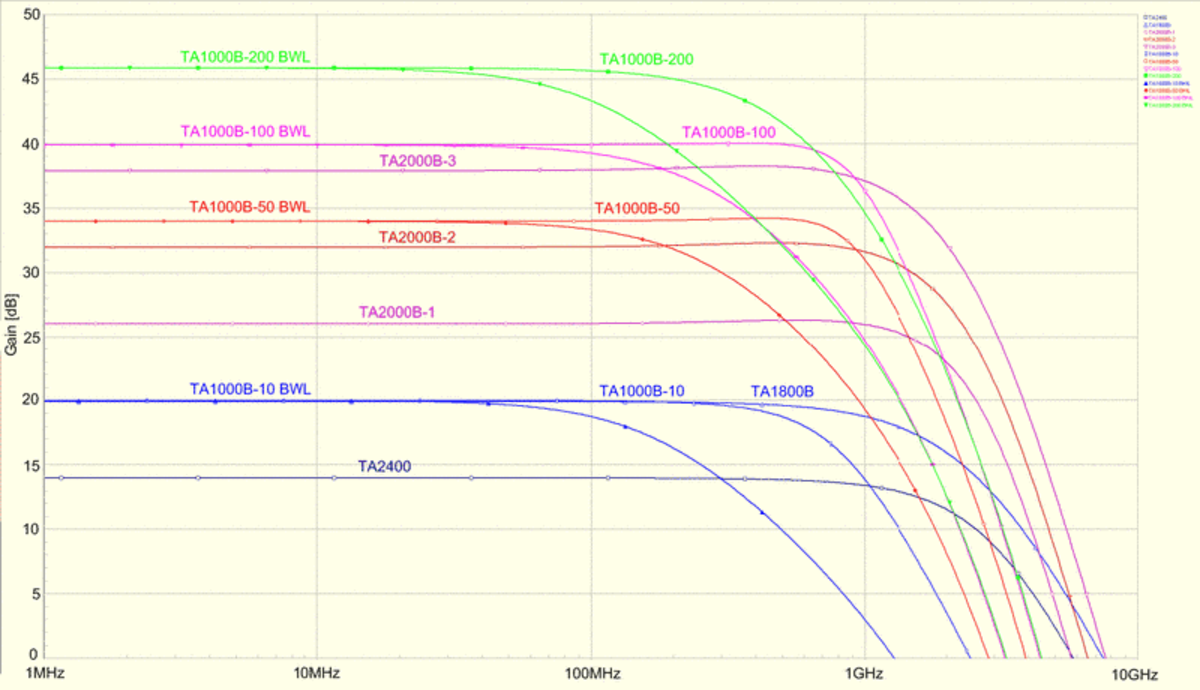
- Voltage gain 20dB (x10), 34dB (x50), 40dB (x100) and 46dB (x200)
- DC coupling
- Closed loop OP-Amp design
- Very low noise
- High output drive
- Single supply operation / internally generated
- bipolar supply / internal supply regulation
- Bandwidth limited (BWL) option available for
- further improved noise performance
- APPLICATIONS
- Pre-amp for ultra fast detectors (MCP, PMT, …)
- Oscilloscope and transient recorder pre-amp
- Photon-/Ion- counting
- Wideband signal processing
APPLICATIONS
- Pre-amp for ultra fast detectors (MCP, PMT, …)
- Oscilloscope and transient recorder pre-amp
- Photon-/Ion- counting
- Wideband signal processing
DESCRIPTION
The TA1000B-x models are fast, very low noise pulse pre-amplifiers with a small signal bandwidth of 400MHz … 1.0 GHz depending on the model.
Each model is av ailable with a bandwidth limited (BWL) option which f urther reduces the noise floor.
A unique feature for such high speed amplifiers is the DC coupling. DC coupling avoids count rate effects due to non DC balanced pulse trains and the corresponding charging of coupling capacitors.

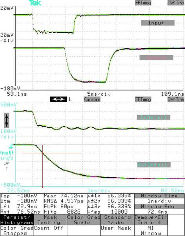

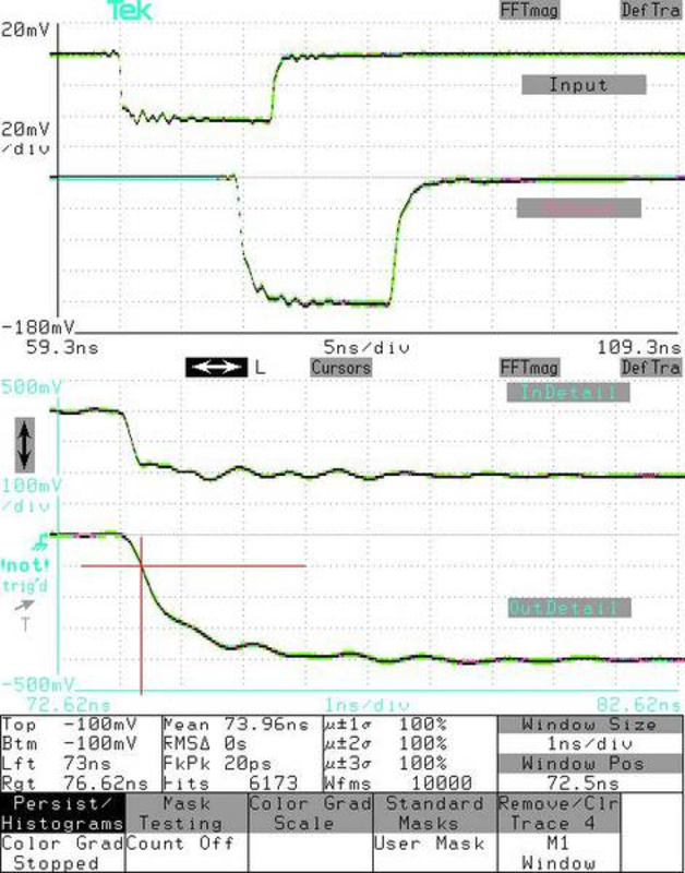

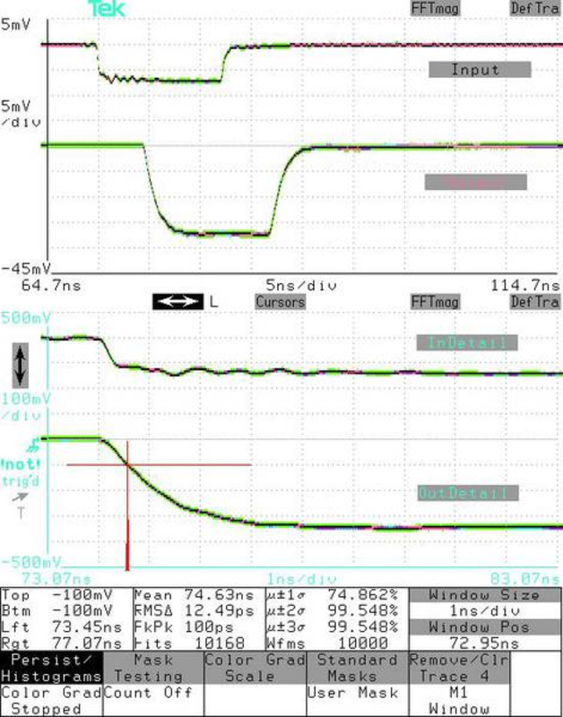
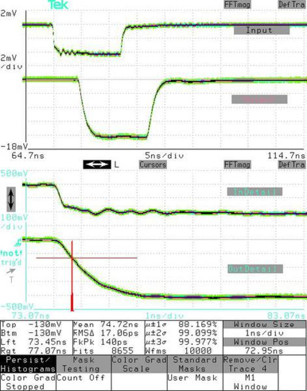
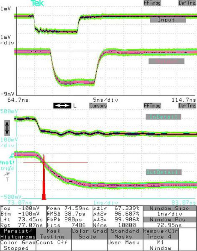
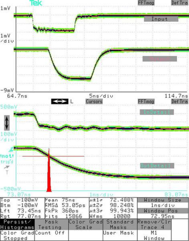
In the following scope pictures you see the pulse response for negative output signals starting at 0V and falling down to –400mV. The input pulse amplitudes are selected according the gain of each amplifier.
The lower window of each plot shows details of the corresponding signals in the upper window. There is also a (redcolored) histogram of the output signal jitter at a-100mV or –130mV threshold. The jitter's Peak-to-Peak value is visible at "PkPk" and its standard deviation in the "RMSΔ" readout.
This jitter histogram gives a good indication of the timing accuracy and resolution that can be expected. And, one can very well see that the optimum threshold setting for timing measurements is often not at half of the signal's amplitude but at some other level not too far from idle voltage where the slew rate is at maximum.
Max. Output Noise Voltage
Normally the noise is given input referred, so to speak, it can be compared to the source signal levels. For timing applications it is often more depicting to plot the total output noise of an amplifier.
In the following scope pictures the output noise voltage of our TAx-amplifiers is accumulated over 10,000 waveforms corresponding to about 40 minutes of measurement time. Used was a TEK11801C digital sampling scope with a 12.5GHz sampling head. Thus, the displayed noise voltage is accumulated over a long period and also over the full bandwidth of each amplifier. The TAx's inputs were shortened, i.e. ZSource = 0Ω.
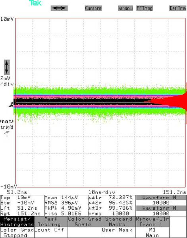
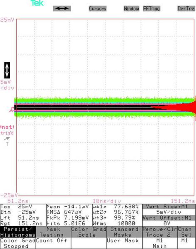
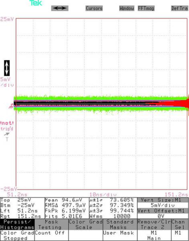
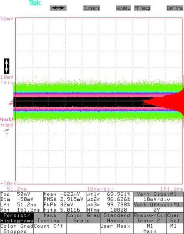
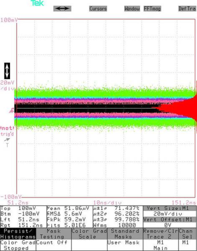

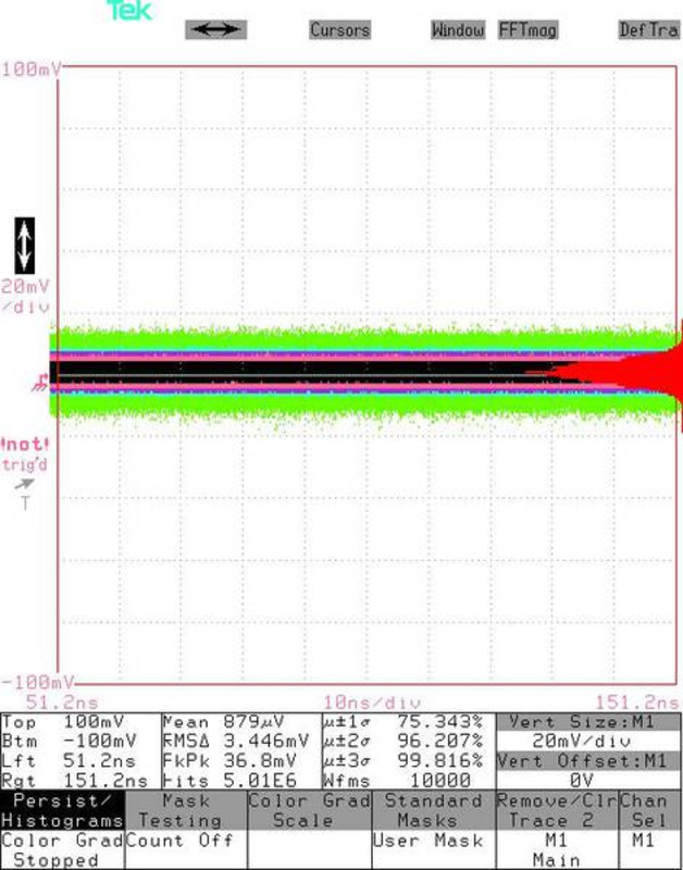
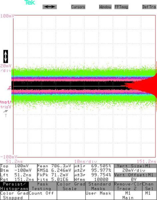

On the right side of each plot you can see a (red colored) histogram of all the voltage samples in the respective picture. This gives the probability distribution of the noise voltage levels. And, you can find some analysis data on the respective voltage distribution: Mean = average value, RMSΔ = σ = standard deviation, PkPk = Peak-to- Peak voltage = max. – min. sample voltage, μ ± 1σ = percentage of samples that fall within ±1 standard deviation of the mean (.±2σ, ±3σ respectively).